
Sony has announced that it has developed a 1.46 megapixel back-illuminated CMOS image sensor that allows for Global Shutter function. While the effective megapixel count might seem inconsequential, it’s far from trivial. This is, unequivocally, a big deal.
The Global Shutter functionality that this achieves has a great many potential benefits in photography, and benefits we have not really had with the switch from CCD to CMOS. Global Shutter tech would allow for the elimination of rolling shutter, most banding, and provide really fast flash sync speeds, among others.
It would seem prudent to mention here that it’s a common misconception that there aren’t CMOS sensors with circuitry that enables Global Shutter. Professional cinema cameras like the Sony PMW-F55 CineAlta 4K, Blackmagic URSA and others are so equipped – but it’s not common, whereas the lion’s share of CCD (charge-coupled device) sensors did/do function with global shutter scanning.
[REVIEW: Sony A9 Review / Overview | The Affirmation Of Mirrorless & Wish Fulfillment]
However, even with the benefits of Global Shutter, less distortion and high QE (Quantum Efficiency), CCD sensors traditionally tend to use significantly (read: exponentially) more power, have much slower data-throughput rates in comparison to those of CMOS (this partially explains why medium format cameras don’t have a high continuous frame rate). CCD sensors also don’t use traditional manufacturing whereas a CMOS sensor can be manufactured in a more typical silicon production line, making them all the more inexpensive and quicker to develop and manufacture. This is, arguably, why they’ve been the go-to.

The shift from CCD technology to CMOS sensors was a boon for overall industry escalation, but like everything else it came with compromise, so having Sony develop a BSI and stacked sensor, something that reduces that compromise, is significant.
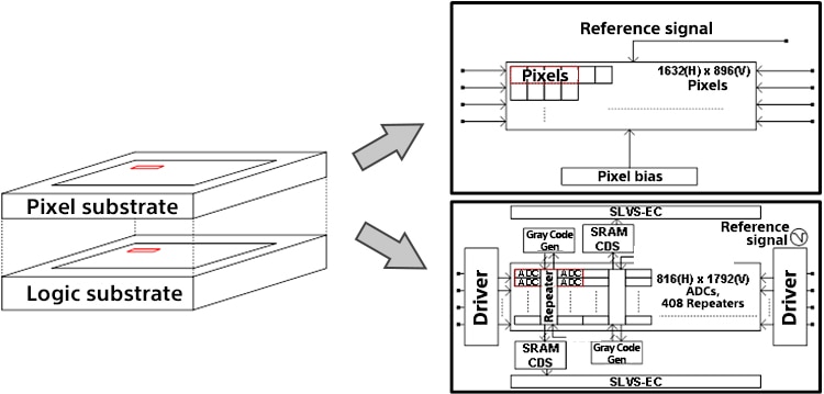
It appears that the primary development here is the number and implementation of analogue-to-digital converters (ADC), which Sony claims is 1000x more than would be found in a normal sensor of its size. So here, the top layer of the sensor has all the photosensitive pixels and the bottom layer houses an ADC for each pixel, and what that translates to is the ability to read all the collective data of all pixels at once, instead of in a sequence of lines as normally associated with CMOS.

Thoughts
This new sensor tech was announced at the International Solid-State Circuits Conference (ISSCC) in San Francisco, where it seems year after year Global Shutter tech gets more talk. Last year at the same conference Canon claimed they had figured out sensor with Global Shutter but with improved dynamic range (an area traditional Global Shutter sensors have lacked in), but we haven’t really seen that development.
But this is Sony, and Sony is nothing if not the innovator and boundary pusher in the industry, so my personal opinion on the matter is that rather than being put off by the incipient nature of the technology at this point, I’d bet there will be proper development of the type. When will we see a usable affordable version of it in a camera? Who knows, but I’d wager it’s coming.
See full press release here.


Get Connected!